


软件

产品


Allegro Sigrity Suite Manager工具套件中的时域SI/PI仿真工具SPEED2000 Generator, 可用于电源噪声的时域分析和验证。Power Ground Noise Simulation流程可用于核心电源的动态压降分析,用户可将从Voltus中获取的Die Model ( 带MCP模型连接协议)加载到对应的器件上并直接在PCB板上进行时域瞬态分析。DDR-SSOSimulation流程可用于I/O信号同步开关噪声的分析,下面以该流程为例,对SSN时域分析的方法和流程做简要介绍。
可在SPEED2000 Generator中参考流程,单击Help→Document菜单,参考其中的DDR-SSO Simulation Tutorial 手册。
(1)打开SPEED2000工具界面,单击菜单File - Open..,导入PCB设计文件SODIMM_DDR_ SSN.spd, 选择流程窗口中的Base Mode中的Power Ground Noise Simulation模式,如图2-85所示。(然后设置叠层结构等)该设计是一个笔记本专用的DDR3 SODIMM PCB板,6层设计,DDR数据位宽为64位。我们利用该案例分析所有DDR数据位做动态随机翻转时的SSN噪声。
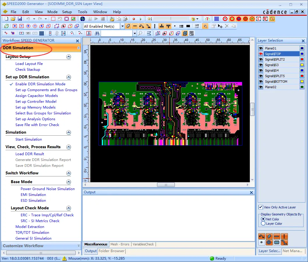
图2-85 SSO/SSN仿真分析流程
(2)单击Set up Components and Bus Groups,弹出向导窗口。利用向导逐步设置元器件(选择Controller和Memory模块)及电源网络及分组。单击Next按钮,定义I/O电源及地网络,并设置VRM工作电压等。
单击Next按钮,设置DDR信号地址、命令、时钟、数据信号网络分组、总线类型等,如图2-88所示。单击Next按钮,确认退出。
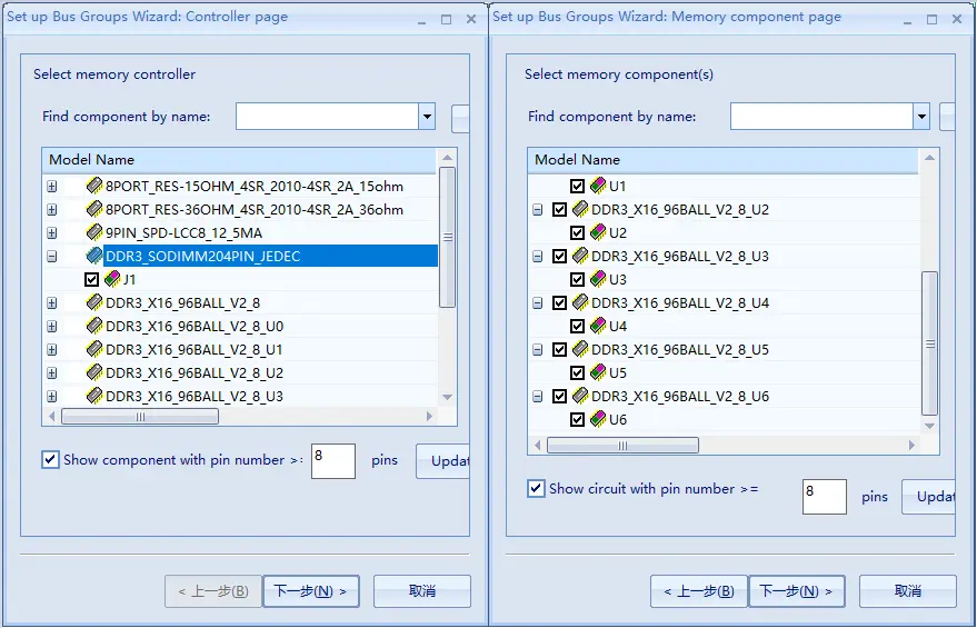
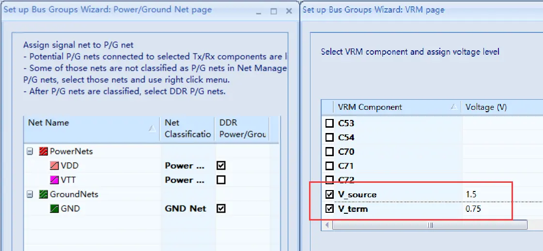
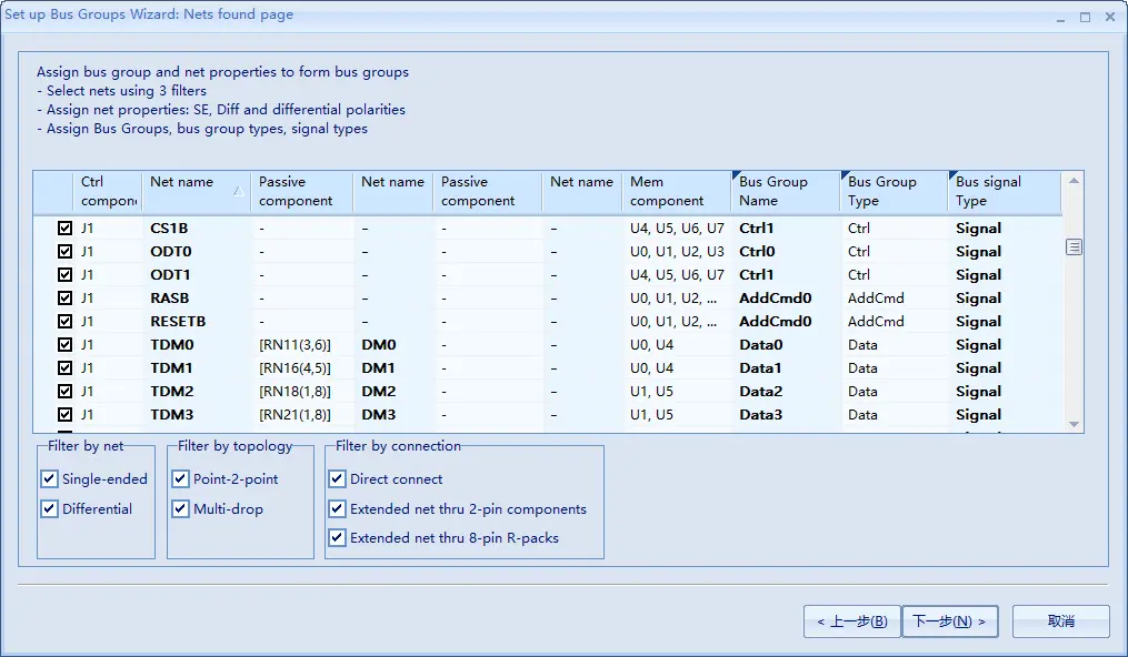
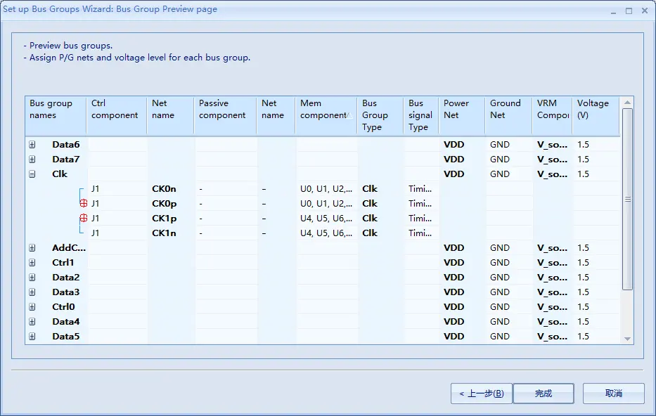
图2-88 选择电源网络及工作电压 设置 DDR信号分组及类型
(3)添加电容模型。单击Assign Capacitor Models,添加板级电容库模型。(或者Setup--->Component Manager---->选择C1---->Edit----->编辑电容模型--->OK(不同容值的都需要添加一次))
可参考DDR-SSO Simulation Tutorial手册。
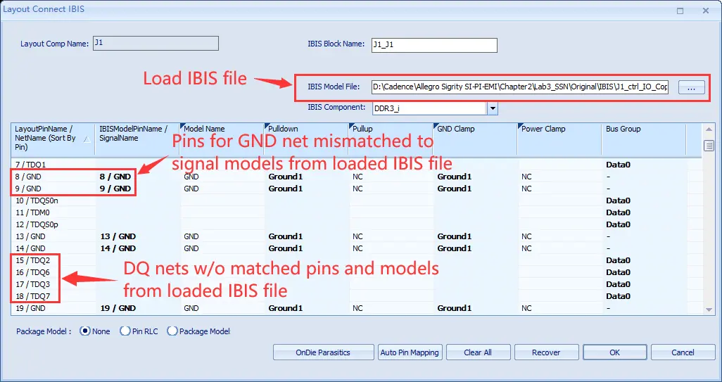
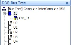
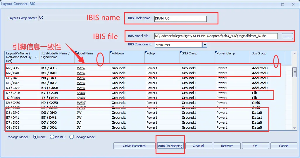
(4)Set up Controller Model,弹出Select Model File -->OK(或者在DDR Bus Tree的 J1 上右击---->Connect IBIS)。,弹出Layout Connect IBIS窗口加载连接器J1关联Controller端的IBIS模型路径,
--->Click the column of LayoutPinName/NetName to sort nets by net name.
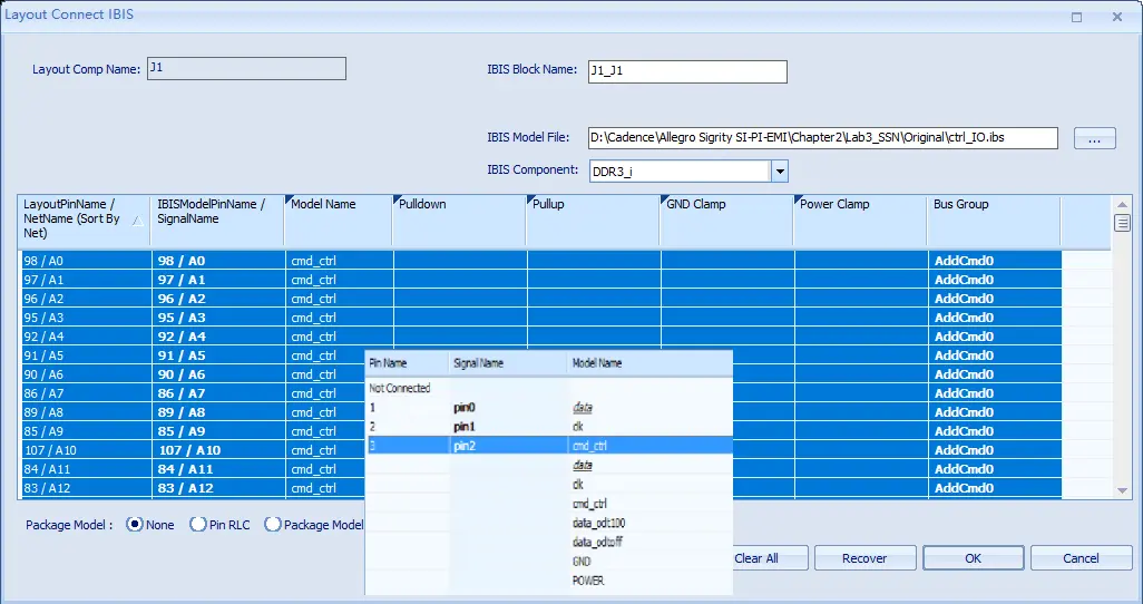
--->To assign buffer model cmd_ctrl to J1 pins for all nets in bus group AddCmd0, in the Model
Name column, choose cells corresponding to nets A0-A15, B A0-BA2, CASB, RASB, and
WEB.
--->Repeat step to assign buffer model clk to J1 pins for nets in bus group Clk.
--->Repeat step to assign buffer model data to J1 pins for nets in bus group data0 and data1.
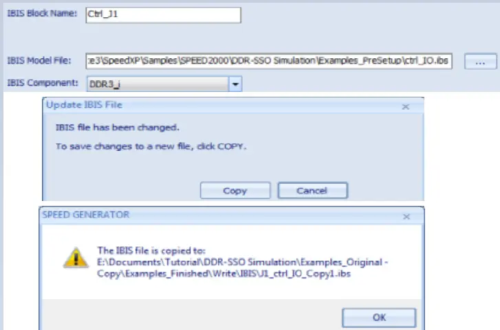
--->SelectJ1_ J1, change the IBIS Block Name to Ctrl_ J1.
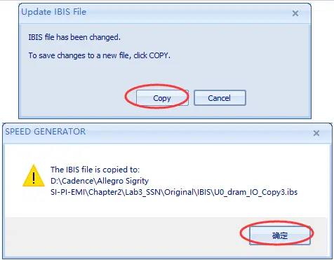
--->Check the newly generated IBIS models and click OK.The Update IBIS File dialog box opens.
--->Click Copy.
--->Click OK to create a new IBIS model. A pin matched component IBIS model for controller J1 is generated, located in the sub-folder named IBIS under the project folder.
The controller IBIS model is shown on the DDR Bus Tree pane.
Set up Memory Model,--->Open the Select Model File Window -->Click OK(或者在DDR Bus Tree的Memeory上右击---->Connect IBIS)。在Layout Connect IBIS窗口中选择IBIS路径及配置
--->Assign buffer model INPUT to U0 pins for nets in bus group AddCmd0
--->Assign buffer model CLKIN to U0 pins for nets in bus group Clk0
--->For bus group Data0 and Data1, assign buffer model DM to nets DMO and DM1; DQS tonets
DQS0n, DQS0p, DQS1n, and DQS1 p; and DQ to the other U0 pins
--->Click Auto Pin Mapping to fill out pin mapping information.
--->Select U0 _U0, change the IBIS Block Name to DRAM_ U0.
--->Check the newly generated IBIS models and click OK.
--->Click Copy. A dialog box opens.
--->Click OK to create a new IBIS model.
A pin matched component IBIS model U0_dram_ I0_Copy1 .ibs for memory component U0 is
generated, located in the sub-folder named IBIS under the project folder.
The DRAM U0's IBIS model is shown in the DDR Bus Tree pane.
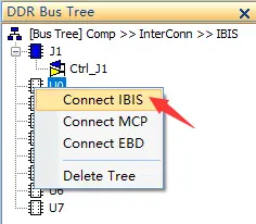
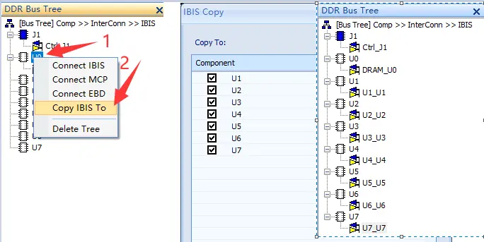
--->On the DDR Bus Tree pane, right-click U0.
--->In the pop-up menu, click Copy IBIS to. The IBIS Copy window opens.
--->Select U1-U7. Click OK.
The DDR Bus Tree pane shows the models copied.
(5)单击Select Bus Groups for Simultion,在最下方的Bus Groups中选择要仿真的网络组。
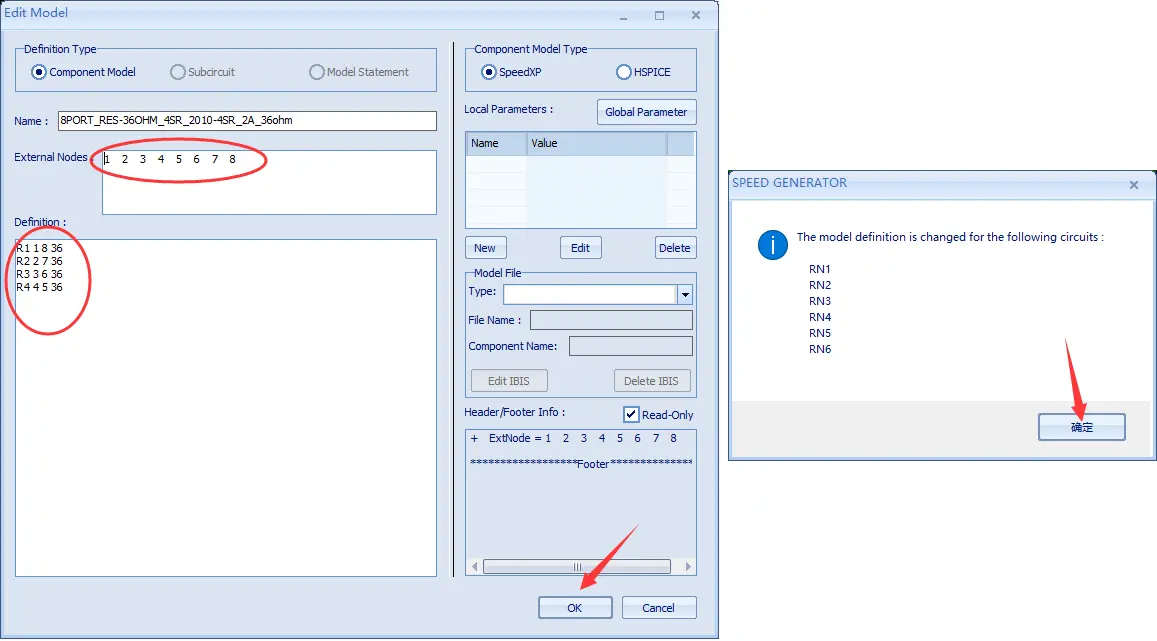
(6)单击Setup Analysis Options, 弹出Analysis Options对话框,设置DDR信号读写方向、信号速率、I/0模型、激励码型等,如图2-89所示。收、发芯片的芯片级去耦电容分别估算为2.0nF和0.5nF。为模拟最恶劣的SSN噪声,激励信号码型被定义为50%占空比的时钟码型,同时所有的64位数据信号做同步翻转。
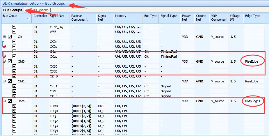
●For Data bus groups, the default Edge Type is BothEdges
●For AddCmd and Ctrl bus groups, the default Edge Type is RiseEdge
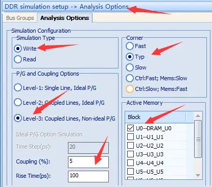
●Select Write for Simulation Type.
●For P/G and coupling Options, choose Level-3: Coupled lines, non-ideal P/G,
。The Coupling (%) and Rise Time(ps) are enabled.
●Set the two parameters as Coupling(%) : 5 and Rise Time(ps): 100.
●Select Typ for process Corner.
●Select U0 as Active Memory (uncheckU1-U7).
Stimulus and Models
1. Set up stimulus on the Ctrl_ J1 tab as shown:
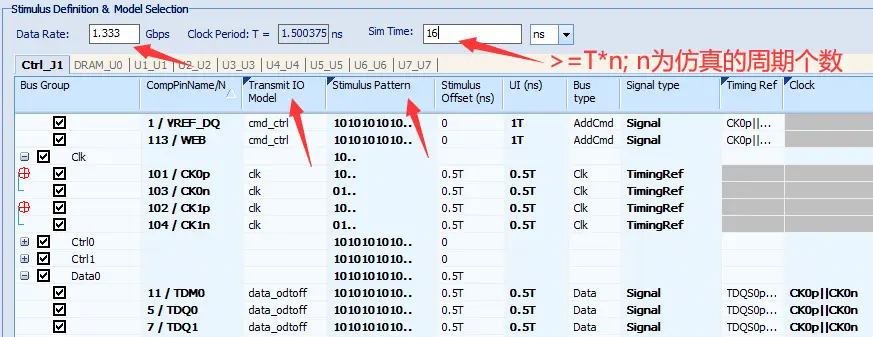

Data rate: 1.333Gbps #ofbits:10 Sim time: 10ns Stimulus for all BGs: 1010101010
2. Set up Ctrl_ J1 models as follows:
AddC md0: transmitter I0 model= cmd_ ctrl
CIk: transmitter I0 model= clk
Data0: transmitter I0 model = data_ _odtoff
3. Set up DRAM_ U0(active memory) models as follows:
AddCmd0: receiver I0 model = INPUT_ 1333
CIk: receiver I0 model = CLKIN_ 1333
Data0: receiver I0 model = DM_ INPUT_ 1333 for DMO, DQS_ 34_ 1333 for DQS0n and
DQS0p, and DQ_ 34_ 1333 for other nets
4. Set up U1_ U1, U2_ _U2, U3_ U3models as follows:
AddCmd0: receiver I0 model = INPUT_ 1333
Clk: receiver I0 model= CLKIN_ 1333
5. Set up U4_ U4models as follows:
AddCmd0: receiver I0 model= INPUT_ 1333
Data0: receiver stby model = DM_ ODT60_ 1333 for DMO, DQS_ 34_ ODT60_ 1333 for
DQS0n and DQS0p, and DQ_ _34_ ODT60_ 1333 for other nets
6. Set up U5_ U5, U6_ _U6, U7_ _U7models as follows:
AddCmd0: receiver I0 model= INPUT_ 1333
△TimingRef is guessed out automatically. You can change it from the drop-down menu.
The Clock column is enabled only for Data bus groups.
7. Click the Save Analysis Options button.
8. Check the nets selected for DDR simulation in the Net Manager.
Termination Resistors for Address Nets
Address nets are terminated to VTT using 8-pin resistor pack. These R-packs need to have valid
model setup to ensure correct simulation results.
1. Launch Component Manager by selecting。 Setup > Component Manager....
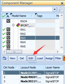
2. Select component RN3, then click Edit.
3. In the Edit Definition window, input circuit model as shown.
4. Click OK. The SPEED GENERATOR dialog box opens.
5. Click OK. The Enable related Circuits dialog box opens.
7. (Optional) You can check the components in Component Manager.
Save .spd Files and Start Simulation
When all settings are complete, you can:
1. Click Save File with Error Check in the Workflow pane to save the .spd files.
2. Click Start Simulation in the Workflow pane to run simulation.
View Results
Waveforms for Data0 at DRAM U0 are shown below.

(7)单击Save File with Error Check保存工程文件和设置,然后单击Start Simulation开始仿真,仿真结束在波形窗口选择查看DRAM颗粒的VDD管脚电压波形。
由于上述仿真假定所有的DDR3数据信号按时钟码型同步、同相位翻转,所以此时信号电流跳变的速度最快,PDN.上电流变化率最快, 其SSN噪声幅度也是最大的。实际上,在DDR信号工作时,随机码型通常更接近于数据信号真实的翻转状态。图2-91为64位数据信号按随机码型做同步开关输出时,U0~U3 器件的电源管脚观测到的SSN噪声波形,其峰值下降为102mV左右。
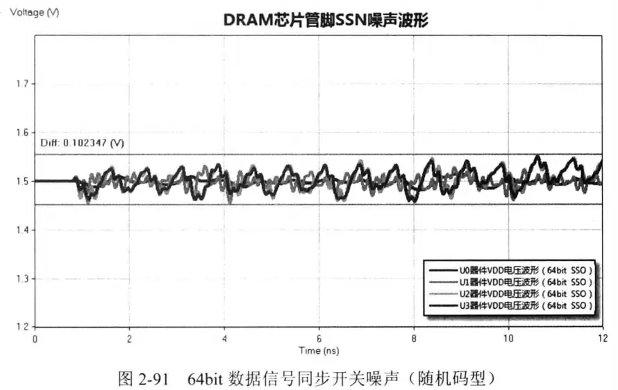
SSN噪声幅度除与PDN的阻抗有关之外,与信号码型假设也有明显关系。有经验的工程师会采用伪随机码( Pseudo Random Binary Sequence, PRBS)或特定设计码型来分析SSN。此外,为提高SSN仿真的精度,用户还需对芯片封装和On-Chip的DDR网络进行准确建模,并采用更高精度的I/O缓冲器模型(如IBIS5.0)。
综上所述,面对当今越来越复杂的PCB设计,Cadence Allegro Sigrity仿真工具套件中的PowerSI和SPEED2000为用户提供了精确、高效的PCB板级和系统级电源完整性解决方案。作为专业的频域和时域电磁场仿真工具,其独特的电磁场模式分解技术为用户在求解包含大量过孔、走线及不规则电源平面等复杂结构时提供全波分析的精度,而自适应的网格剖分技术和智能的多CPU、多线程处理技术将极大提升仿真效率。而其简洁、流畅的流程化设计,使得无论是硬件设计工程师还是电源完整性工程师,都能快速利用该工具解决在项目开发中面临的诸如阻抗控制、谐振分析和抑制、去耦优化、SSN噪声分析等挑战,提前发现设计缺陷,提升产品设计质量和可靠性,并加快产品上市时间。
Generate DDR Simulation Report
This chapter introduces how to generate DDR Simulation Report. Write mode is taken as an example in below illustrations.
1. To generate a report, click Generate DDR Simulation Report in the Workflow pane.
The Select Additional License window opens.
2. Select the desired additional license. (Check all the three licenses in this example.)
3. Click OK. A message dialog pops up to confirm the findings.
4. Click OK. The Generate Report window opens.
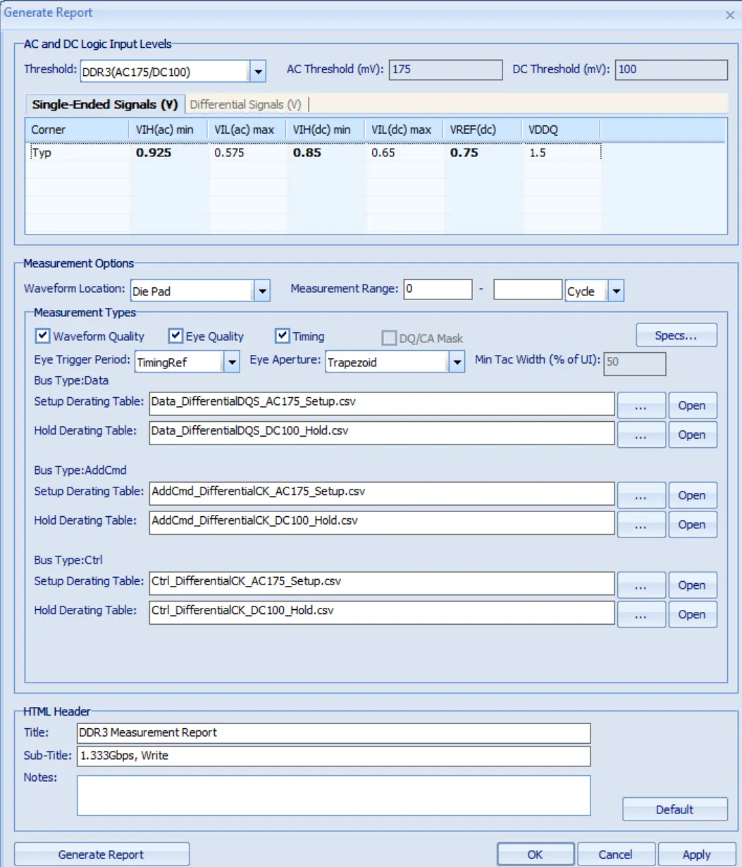
The various parts of this dialog box are discussed below:
Threshold - JEDEC specific AC and DC threshold levels for known DDR1, DDR2, DDR3,
DDR4, LPDDR2, LPDDR3, and LPDDR4(Class-1) standards are included.
■ Selecting one of these updates the Voltage values in the Dialog, including the AC and DC threshold values, as well as the Single-ended and Differential Typicalcorner values for Low and High logic levels
■ A user-defined threshold can also be created here
Waveform Location - Die Pad is selected.
Measurement Range - It is specified by user.
■User can choose anyone of the three units: ns, ps and Cycle.
Measurement Types - The Measurement types currently include Waveform Quality, Eye Quality, Timing and DQ/CA Mask.
■DQ/CA Mask is enabled only for DDR4 and LPDDR4 measurements in the Write simulation type. It will be grey if DDR4 or LPDDR4 is not selected or in the Read simulation type
■When DDR4 is selected, only Data bus can be measured by waveform quality and DQ/CA mask
■When LPDDR4(Class-1) is selected, AddCmd, Ctrl and Data buses can be measured by waveform quality and DQ/CA mask
■When DDR4 or LPDDR4(Class-1) is selected, Eye Quality and Timing are grey
Specs - Spec parameters are defined here by bus type. The Usage tD*_ * is for the Data bus type, and tl*_ * is for other bus type.
Click the Specs... button to open the Specs window. You can edit the parameters. In this tutorial, just keep the default values.
There are four types of Spec groups:
■Timing: Enabled when Timing is selected. P arameters in this group are applied on the bus types selected
■When only Data bus is selected, it shows two rows named tD*_ *
■When only other buses are selected, it shows two rows named tl*_ *
■When both Data bus and other bus types are selected, it shows four rows, two rows named tD*_ *, two rows named tl* _*
■Timing - Strobe and Clock: Enabled when Timing is selected and Data bus is selected. P arameters in this group are applied on the Data bus type
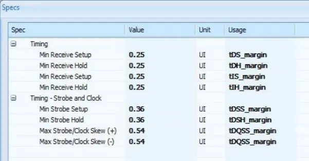
■DQ Mask: Enabled when DDR4 or LPDDR4 is selected. Parameters in this group are applied on the Data bus type
■CA Mask: Enabled when LPDDR4 is selected. Parameters in this group are applied on the other bus types except Data

Eye Trigger Period - You can choose TimingRef or Same As UI. It is TimingRef by default.
Eye Aperture
■Two options are available for Eye Aperture:
■Trapezoid - Selected by default
■Tac/Tdc Rectangles一 If selected, eye mask consists of two rectangular shapes: .
■Tac: Height of 2*VIH(ac)(from VIL(ac) to VIH(ac)), with a width of Tac.
■Tdc: The second rectangle is from (VIL(dc) to V lH(dc)) and with width of Tdc.
The overall eye aperture width measurement=' Tac + Tdc.
Min Tac Width - Can be useful when TacTdc Rectangles is selected for Eye Aperture.
■Itis a positive number ranging from0 to 100.
■The default value is 50.
Derating Tables - They are loaded automatically according to the Threshlold selected.
The tables are classified by the bus group, and are only enabled when the corresponding
bus group types(Data, AddCmd, and Ctrl) exist.
You can also select the derating tables manually by clicking the browse button. The default
location for the derating tables is in the Allegro Sigrity installation directory, typically: .
<Sigrity_ install gdir>lsharelLibraryltemplatelSPDGENlDeratingTable\
5. Specify the following parameters as described below:
Threshold: DDR3(AC 175/DC 100)
Measurement Range: 2-8 cycle
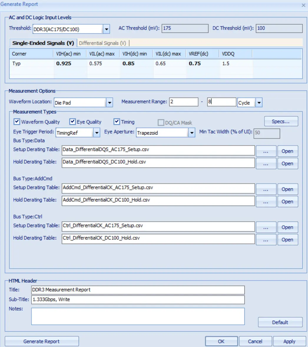
6. Click Generate Report to start to generate the report.
7. To save the report, click Save DDR Simulation Report in the Workflow pane.
武汉格发信息技术有限公司,格发许可优化管理系统可以帮你评估贵公司软件许可的真实需求,再低成本合规性管理软件许可,帮助贵司提高软件投资回报率,为软件采购、使用提供科学决策依据。支持的软件有: CAD,CAE,PDM,PLM,Catia,Ugnx, AutoCAD, Pro/E, Solidworks 等。
 技术文档
技术文档
 推荐好文
推荐好文


 155-2731-8020


