


软件

产品


PCB Editor 17.4 导入其他 EDA 系统(e.g. AD)的pcb文件, 转换成自己的格式。
然后再将库导出到其他目录时,可以看到有单独的焊盘.pad文件。
很好奇这些焊盘文件的命名方式,去查了一下。
看到SPB官方帮助文件为 file:///https://www.gofarlic.com/Cadence/SPB_17.4/doc/algrologic/chap3.html
Transferring Logic Design Data
Padstacks
Padstacks are one of the most difficult items to convert because of the many ways other systems store pad information. Other converters have to derive the library padstacks from the pad uses within the package symbols. All other converters require a program-manufactured name.

The algorithm that defines the name is as follows:

The name begins with the width of the top pad, followed by the letter C (circle) or S (square).
If the pad is rectangular or round, it is followed by an X and the top pad height.
The bottom pad follows the top pad and uses the same format. The hole size and plating are last.
The letter P indicates the hole is plated. (All sizes are in mils.)
The following name represents a padstack with a 50 mil top pad and a 50 mil bottom pad, and a 28 mil plated hole:

50C50C28P.pad

The following name represents a padstack with a 25 x 100 mil pad defined only on the top:

25X100.pad

Since the name only depends on the top and bottom pad definitions, you would get the same name for the padstack if the only thing different was the inner pad definition. In that case, the pad name would be modified to be 50C50C28P.pad and 50C50C28P_1.pad.

If the naming convention does not match the naming conventions you use, you can rename them. Just remember that symbol-building scripts require a padstack with the name defined by the converter. You have two ways to get around this. One is to keep the padstacks the way they are and create the ones you want and use a replace padstack in the symbol editor. The other way is to fix the symbol-building scripts to call for the padstack name you defined.

Whether you choose to keep the name the same, you should check and modify the padstack to your standards. Some converters do not consider thermal and anti pads because the older system did not define them the way they are defined in the layout editor. You should also select the drill shape. You should be familiar with the padstack documentation. These correct padstacks should be put in the master padstack library established by your system manager.
这段官方说明和实际自动导出的.pad命名,并不完全一致。但是能看出些东西出来了。
具体命令,还是要打开具体导出的.pad, 对照参数看一下,就能清楚。
看了一些第三方资料,号称xx公司PCB规范,但是其中的焊盘命名规则很不规范。
所以说,看规范,还是要按照大厂的来才靠谱。
SPB官方这种焊盘命令规范,可以最大程度降低焊盘命名的重复性,而且见名知义。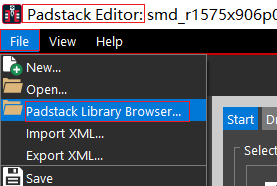
单位mil, 精度2位
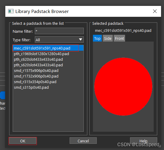
通孔,圆形焊盘
这是一个纯的钻孔(机械孔), 表示为 mec
焊盘尺寸 圆形 59.06 x 59.06 进位后表示位 c591, 其中c代表圆形,591 = 59.1mil
钻孔槽形状为59.06 x 59.06, 进位后为59.1 表示为 slot591x591
阻焊层尺寸 = 圆形 67.06mil
67.06(阻焊尺寸) - 59.06(焊盘尺寸) = 8(直径上的2个阻焊环宽度) /2 (2个阻焊环) = 4mil = 4.0mil => s40
np没看出代表啥。
从这个例子 mec_c591slot591x591_nps40.pad 猜读规则
焊盘类型(机械孔mec,通孔焊盘pth,表贴焊盘smd)_焊盘尺寸(cyyy,其中c位圆形,s位正方形,r为长方形 焊盘尺寸)_钻孔槽尺寸(slotyyy_zzz)_np(未知,暂时猜读为没有(no)焊盘(pad))_s40(阻焊宽度).pad
pth 通孔焊盘
c圆形焊盘 焊盘尺寸为196.85 进位保留1位小数点 为196.9 => c1969
钻孔槽尺寸 = 127.95 x 127.95 进位保留1位小数点 为128.0 x 128.0 表示为slot1280x1280
阻焊层pad 为圆形 204.85mil, 进位保留1位小数点 为2049
2049 - 1969(焊盘尺寸) = 40 => s40 说明 s为阻焊层 40为阻焊层宽度为40mil
从这个例子 pth_c1969slot1280x1280s40.pad 猜读规则
焊盘类型(机械孔mec,通孔焊盘pth,表贴焊盘smd)_焊盘尺寸(圆形焊盘 196.9mil直径)_钻孔槽尺寸(slot 128.0mil x 128.0mil)_阻焊环宽度(s_40mil).pad
pth 通孔焊盘
c620 圆形焊盘 焊盘直径62.0mil
slot433x433 钻孔槽尺寸 = 43.3mil x 43.3mil
s40 = 阻焊宽度 = 4.0mil
pth 通孔焊盘
s 正方形焊盘 焊盘尺寸 = 62.0mil
slot 钻孔槽尺寸 = 43.3mil x 43.3mil
s40 阻焊宽度4.0mil
smd 表贴焊盘
r 长方形焊盘 尺寸 = 157.5mil x 90.6mil
p0 只在顶层有焊盘(暂时猜读 p1为底层有焊盘 p2 为顶层和底层都有焊盘)
s40 阻焊宽度 = 4.0mil
同上,没有不同。
smd 表贴焊盘
s 正方形焊盘 焊盘尺寸 = 31.5mil
p0 只在顶层有焊盘
s40 阻焊宽度4.0mil
smd 表贴焊盘
o 代表椭圆形(oblong)焊盘 焊盘尺寸 24.8mil x 73.4mil
p0 焊盘在顶层
s40 阻焊宽度4.0mil
通过阅读官方文档,通过猜读和实验,已经看懂大部分焊盘命令规则。
如果遇到新的焊盘命名规则再补充。
如果器件是第三方库(e.g. AD or Footprint Expert)引入的,可以用cadence导出库的功能,再对焊盘自动命名1次,这样焊盘的命名规则就一致了,且不易重复。
如果真的看到焊盘命令有重复(因为我就一个统一的焊盘库路径,新元件进来时,会将导出的库手工拷贝进来,那样,如果有重复命令的焊盘文件,就会有提示),可以用Padstack Editor 17.4打开焊盘文件, 就那几个界面(焊盘形状,钻孔尺寸,焊盘尺寸,阻焊宽度,焊盘在哪层?),看看到底有啥不同。如果真有不同,也可以参照SPB官方的命名法,将不同的地方加上不同的新的 关键字 。
不过,我相信,cadence的焊盘命令法是不会出现重复的(前提是,2个焊盘确实不同)。用的焊盘多了,就知道了。也期待能看到SPB官方命名法有重复的例子。
不过,我想大厂应该都将不重复命名的问题都考虑到了(设计者应该能考虑到使用者将所有焊盘都放到一个目录的情况),要想知道具体啥样的焊盘设置会引起命名重复,我们也没有cadence实现的代码,只能去逆向SPB17.4焊盘自动命名这部分实现才知道(有点扯远了)。
免责声明:本文系网络转载或改编,未找到原创作者,版权归原作者所有。如涉及版权,请联系删
 技术文档
技术文档
 热门文章
热门文章


 155-2731-8020


